


Signal Integrity Analysis
AEi Systems has a new, super-fast Signal Integrity Analysis Service for all types
of digital circuitry, which is especially applicable to space and high-reliability
applications.
The "BOARD CHECKOUT" package is an EXHAUSTIVE validation of your board, layout,
and interconnect performance. It includes the following analyses:
• Signal Integrity
• DC Interface Compatibility
• Decoupling
• FPGA SSO
• Critical Timing Relationships (WCTA)
• Crosstalk/Ground Plane Coupling
• Power Sequencing
• PDN and Power Systems Assessment
Signal Integrity Analysis - Signal integrity (SI) analysis is an essential part of evaluating most of today’s board designs. Increasingly, fast edge rates and design complexities in high speed (> 10MHz) PCBs impact performance in sometimes unseen ways. As ICs switch faster, designs suffer from signal degradation, including over/undershoot, ringing, glitching, crosstalk, and timing problems, which all must be accounted for along with the physical PCB implementation. A thorough and rigorous analysis is the only way to validate that a successful outcome is likely. With the help of our Logic Command software AEi Systems can perform these analyses quickly and cost effectively.
Signal integrity analysis consists of series of analytical task intended to verify reliable communication between all digital circuits on a board. The analog/power/non toggling bias nets, digital data nets and clock net are analyzed. Critical edge-detect (of potential edge-detect) signals must be identified and analyzed to guarantee that their transitions will be monotonic for the life of the mission. Overshoots and undershoots occurring while transitioning between states must be reduced to a safe level guaranteed by the specification or other reliability criteria. Items Considered During a Signal Integrity Analysis
Items Considered During a Signal Integrity Analysis
- • Characteristic impedance of PWB
- • IBIS model performance range exhibited by the Slow, Typical, and Fast versions
- • Propagation delays
- • PWB characteristic impedance and material
- • Package and die parasitics
- • Vias
- • Input capacitance to the ASIC and ICs
- • Pin contact inductance
- • Connecting wire between boards
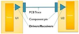
DC Interface Compatibility Analysis - An interface analysis validates that each interface meets the output and input requirements to perform a given function. In digital circuits, a good example is to validate that TTL outputs are joined with TTL compatible inputs, and that the fanout requirements are met.
Example of Interface Compatibility report diagram, showing all of the components taken into account. Supply and ground noise, leakage currents, clamp diodes, package pin resistances, and driver impedance.
Decoupling Analysis - The objective of this analysis is to determine the
adequacy of the external decoupling and estimate the switching noise levels inside
of the ICs on the board. It also confirms that the local power supply decoupling
noise is less than a designated amount for all drivers/receivers. Noise at the IC
due to imperfect local decoupling and internal noise due to simultaneously switching
outputs are also assessed. All of the ICs on the board are divided into basic and
complex devices. Basic ICs have a limited, for instance, a device with eleven (11)
SSOs that sink or source 5mA with a rise or fall time of 900psec will have better
decoupling performance than one with nine SSOs that sink or source 50mA with a rise
or fall time of 1nsec. Each device is reviewed, a determination made, and the rationale
explained. Review the component datasheet and application notes (if applicable).
The design is also checked to see that manufacturer’s layout guidelines are followed.
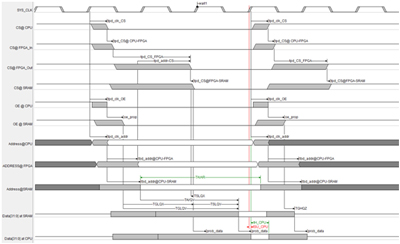
Worst Case Circuit Timing Analysis (WCTA) - The digital worst case timing
analysis (WCTA) portion of the WCCA analyzes the timing of digital devices and signal
paths under worst case conditions. For the WCTA, the results of the board propagation
delay and the static timing numbers of the FPGA or ASIC are analyzed by TimingDesigner.
It is through the use of TimingDesigner’s advanced plotting capabilities that violations
can be seen. In the digital WCTA, both rising and falling edges of the slow and
fast cases are examined for timing board propagation delay.
Here is a link to a sample SI/PI analysis:
•
Sample SI/PI Analysis Report
What this download includes:
• Signal Integrity
• Crosstalk
• Logic Compatibility
• WC Timing
• Power Sequencing
Note: Must be U.S. Citizen to receive this ITAR information
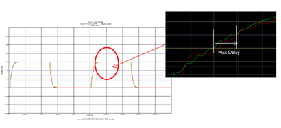
Example of the Timing simulation waveform to measure the board propagation delay.
The difference between these two propagation delay is used as an adjustment factor,
which is applied to the propagation delay that is calculated by FPGA/ASIC design
tool.
The results of the 8Mbytes SRAM read timing analysis with one wait state as an example of the digital worst case timing analysis. As shown above, the CPU setup time requirement is not met under the worst case conditions.
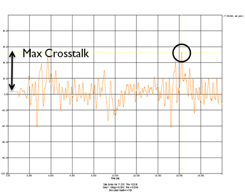
Cross-talk Analysis computes the nominal and worst case crosstalk caused by interference between traces, between all possible combinations of aggressor/victim signals. The basic concept of crosstalk can be described as a fast transition on one or more signals, called “aggressors,” which are coupled onto nearby signals (“victims”). Each signal is expected to be in a certain voltage range for proper operation. If the induced voltage exceeds a certain maximum value, sufficient to bring the signal level into the threshold range, a functional failure may occur. Some small levels of crosstalk are unavoidable in any practical digital design and must be simply accounted for in noise margin budgets for all signals. For a board analysis, the amount of noise generated by crosstalk on each net is used in the DC Compatibility analysis as a margin allocation specifically for the crosstalk. The analysis accounts for the exact geometry of all traces, pads, layer dimensions, etc. The IC I/O models used vary based on the part type, availability of appropriate models from the manufacturer, and other factors.
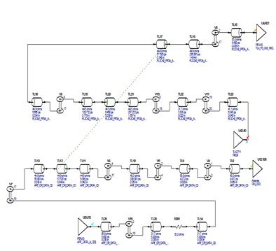
Example of the Crosstalk HyperLynx Simulation Setup.
Example of the Simulation waveform for the couple net shows the 53.05mV as the peak Crosstalk.
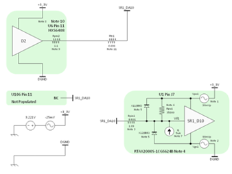
FPGA SSO - The goal of the analysis is to confirm that the local power supply
decoupling noise is less than 250mV on the VDD rail and less than 100mV on the ground,
for all drivers/receivers. The noise voltage is measured locally to the driver on
the die, with respect to a neutral ground far away from the switching effects. Any
droop or bounce greater than these values will cause more findings in the DC compatibility
performance.
AEi Systems has developed a methodology for measuring the worst-case effects of
SSO and carried out laboratory testing using the commonly used part, the Microsemi
RTAX2000. This testing has demonstrated the levels of ground-bounce and VDD-droop
experienced at the die of the device with varying numbers of SSO with various driver
strengths, over a range of operating I/O voltage levels and temperatures.
Analysis | SPICE Modeling | Publications
Home | Services |
About Us | Contact Us | Jobs
Terms of Use | Site Map
©AEi Systems, Inc. All Rights Reserved.